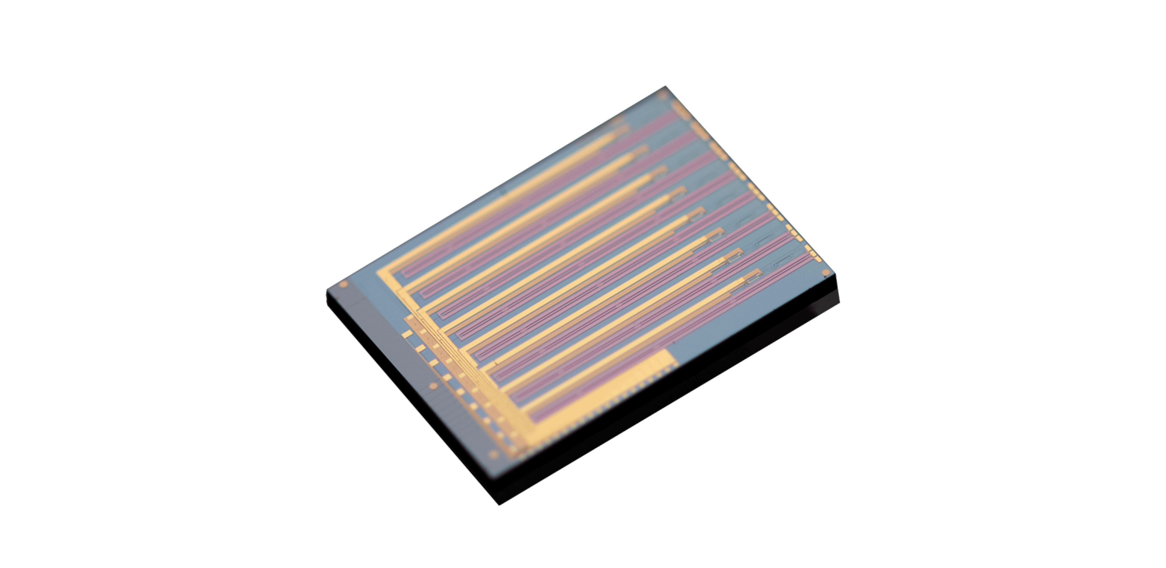
High-speed transmission is limited by both the speed of individual devices and by the connections between them. Long RF traces, repeated optical alignments, and inconsistent discrete assemblies consume margin as symbol rates rise.
They use integration to shorten those paths, improve repeatability, and place related optical functions within a circuit that can be designed and tested as a coordinated unit. Capacity requirements now span dense data-center links, coherent transport, measurement systems, and sensing. Each use case values a different combination of bandwidth, optical loss, voltage, linearity, and channel count.
A successful integrated circuit does not push every parameter to its limit; it balances them for a defined architecture while leaving enough margin for package and system variation. TFLN chips provide one route to high-speed electro-optic integration.
Published products include multi-lane devices for 800G, 1.6T, and 3.2T, a coherent PDMIQ circuit, and a bare intensity-modulator die. They consider this range evidence of possible applications, then evaluate whether each product can be assembled, driven, qualified, and supplied within their program constraints.
Integration Shortens Electrical and Optical Paths
Photonic integrated circuits can combine splitters, interferometers, phase shifters, polarization functions, and several modulation lanes on one substrate. Fewer discrete optical interfaces may improve alignment consistency and reduce the physical path between functions.
Integration provides a return when the package preserves that integration rather than reintroducing long, lossy, or poorly controlled connections around the die. Electrode design is as important as the optical waveguide in TFLN chips. The RF signal must travel with appropriate impedance and velocity while maintaining electric-field overlap with the optical mode.
At 70 or 110 GHz, package transitions and driver connections can restrict usable response, so they co-design the die, interposer, and board instead of treating them as independent purchases. Multi-lane integration also supports compact transmitter architectures, yet it introduces coupling and uniformity challenges.
Every lane must meet an acceptable response and loss range, and fiber arrays must align across the full set. They model the impact of lane variation on module yield because aggregate capacity is limited by the channel that fails its specification, not the average channel.
Link Performance Emerges from Balanced Device Parameters
A 3.2T DR8 product is listed at 110 GHz with differential half-wave voltage below 1.5 V and extinction ratio above 25 dB. These figures influence driver swing and signal quality, while the below-14-dB insertion-loss figure including coupling affects laser power.
Photonic integrated circuits must be assessed through this combined budget, not by bandwidth alone. The 70 GHz 1.6T DR8 or 800G DR4 option has differential half-wave voltage below 2 V with a similar stated loss boundary.
When comparing TFLN chips for a specific module, they simulate actual symbol rates, modulation amplitude, equalization, temperature, receiver sensitivity, and manufacturing spread.
A lower headline rate may still be a closer fit when it provides more practical margin. Coherent transmission changes the priorities. A listed PDMIQ circuit has insertion loss below 7 dB, differential half-wave voltage below 4.5 V, and 70 GHz bandwidth.
Its integrated polarization and IQ functions support complex formats, but the design also needs stable bias, balanced paths, linear drivers, and digital processing. The complete transmitter architecture determines the value of each parameter.
Commercial Deployment Needs a Controlled Manufacturing Ecosystem
Volume deployment begins with a process-control plan for photonic integrated circuits. They request wafer maps, statistical limits, test correlations, lot traceability, and notification of changes to materials, masks, fabrication, or assembly.
These controls help distinguish random module issues from systematic device shifts and allow corrective action before a large number of units reaches the field. Packaging partners must be involved in qualification of TFLN chips because coupling and RF transitions can dominate final performance. They use representative materials, adhesives, fibers, connectors, thermal cycles, and reflow or attach processes.
Reliability evidence from an unpackaged die cannot replace testing of the assembly that customers will operate for years. Production test economics also affect adoption. High-speed multi-channel devices can require expensive instrumentation and long calibration sequences.
They separate required screening from deeper characterization, develop correlation limits, and automate data collection. The objective is adequate coverage at a cycle time that supports the planned volume and preserves useful manufacturing feedback. System partitioning may also shift over time.
Functions initially placed in separate optics, electronics, or firmware can move as integration and control improve. They preserve modular interfaces during early generations so that a later architectural change does not force every adjacent subsystem to be redesigned simultaneously. Integration matters because it offers a way to manage complexity as data rates rise.
By coordinating optical functions and reducing uncontrolled interfaces, it can protect signal margin and enable denser modules. Those advantages become real when electrical, optical, mechanical, and test design are developed together from the beginning.
They recommend evaluating integrated solutions with a system demonstrator rather than a component-scorecard. The demonstrator should report energy per bit, optical margin, error performance, temperature sensitivity, assembly yield, and test time. That evidence links device specifications to the commercial outcomes that determine whether a transmission platform can scale.
Integration creates value when fewer interfaces produce measurable system margin without making test and repair harder. A multi-architecture demonstrator can place Liobate alongside other circuit options and expose that balance under direct-detection, coherent, or sensing conditions.
